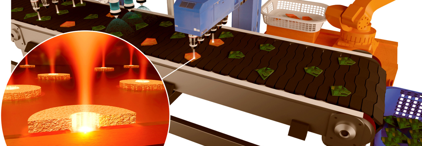
NanosensorID - Optical ultra-sensors to help to recycle various materials, from e-waste to paper
NanosensorID offers materials (plastics, cardboard/paper, metals, glass, e-waste) identification on the spot with hand-held or fully automated/fast scan.
IVAs 100-lista 2023

There are natural limits of how materials can be identified according to their physical properties in recycling process. For example, in e-waste (electronic waste) recycling, $57 billion worth materials end up in the land field from discarded electronics every year. This is 50-60 million tons yearly. These are primarily metals (copper, nickel, tin, lead, gold, platinum, palladium, silver) and various plastics. At the same time, critical raw materials (like metals) content in e-waste is typically higher than in mined ores. But physical modern methods can’t identify and separate them.
NanosensorID offers materials (plastics, cardboard/paper, metals, glass, e-waste) identification on the spot with hand-held or fully automated/fast scan. We use optical nanoplasmonic sensing as a tool to identify materials with close to 100% accuracy. The enabling step is our ability to deposit precisely engineered optical nanosensors onto any surface of choice.
